


")

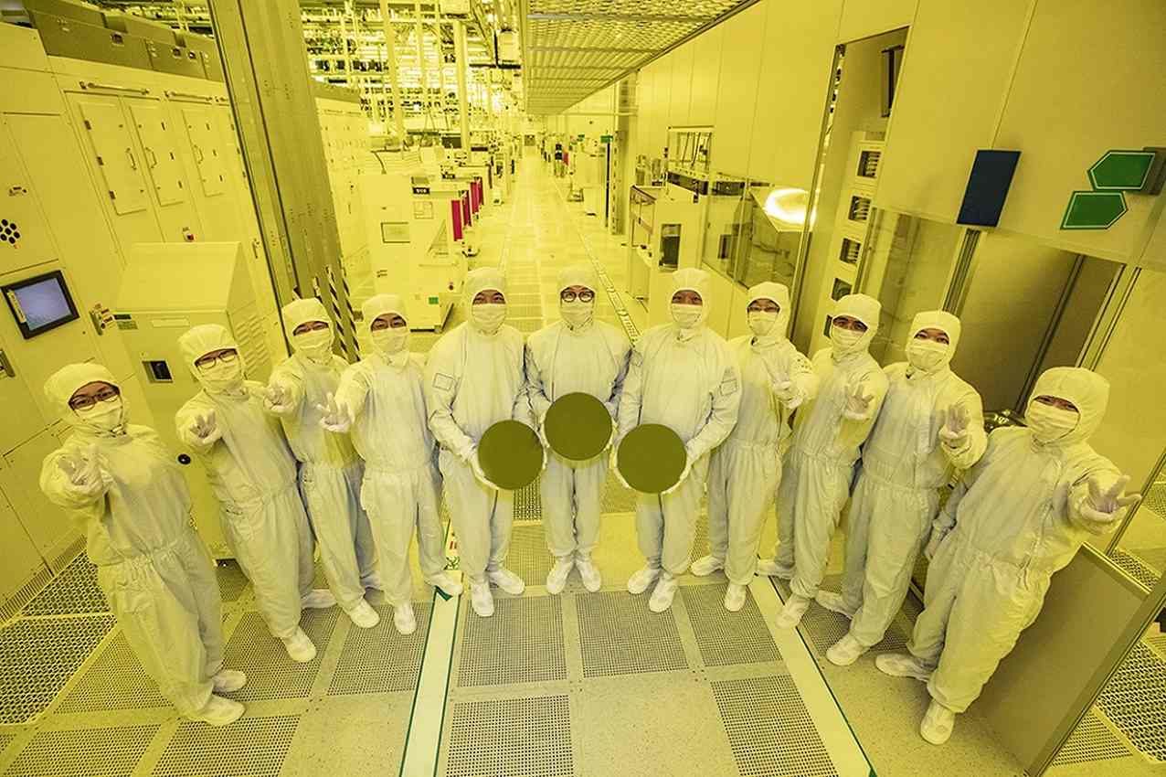
Samsung Electronics announced that it has started initial production of its 3-nanometer semiconductor chips, down from their previous 5-nanometer.
The company is starting the first application of this nanosheet transistor with semiconductor chips for high performance, low power computing application and plans to expand to mobile processors.
Compared to 5nm process, the first-generation 3nm process can reduce power consumption by up to 45%, improve performance by 23% and reduce area by 16%, while the second-generation 3nm process is expected to to improve these even more.
“Samsung has grown rapidly as we continue to demonstrate leadership in applying next-generation technologies to manufacturing… We seek to continue this leadership with the world’s first 3nm process,” said Dr. Siyoung Choi, President and Head of Foundry Business at Samsung Electronics.
“We will continue active innovation in competitive technology development and build processes that help expedite achieving maturity of technology.”
This smaller, more powerful computer chip is the company’s best attempt to compete with the Taiwan market dominance of chips and integrated circuits.
A 3nm chip opens up huge variety of possibilities for tech manufacturers to save space in the circuit boards of their devices, and combined with a mass-production plant they are hoping to have operational in Texas by 2024, Samsung is poised to help along another diminution in device size and price.
As technology nodes get smaller and chip performance needs grow greater, chip designers face challenges of handling tremendous amounts of data to verify complex products with more functions and tighter scaling. To meet such demands, Samsung has said they hope to provide a more stable design environment to help reduce the time required for design, verification and sign-off process, while also boosting product reliability.
SHARE This Big Story About Tiny Tiny Chip…