Inside nearly every piece of electronic equipment, there’s a transistor—a simple component that receives a current and sends it in one or more other directions.
It’s one of those things that deserves an expression like “a new mousetrap,” because if someone were to invent a better one, that would change the industry immediately, to the inventor’s great fortune.
Now that very thing has happened, and a new transistor design could cut the entire world’s energy usage by around 5%, by reducing the number of individual transistors needed to store data by three-quarters.
Millions of transistors line the surface of every modern microchip, which itself is manufactured in staggering numbers around the world, reaching into the trillions. However, the microchip is now reaching the limit of how small it can be made—and with that, how much heat can be dispersed from the electronic demands of modern computing by something that’s only 25 silicon molecules-thick.
Physicist Peter Dowben, the Charles Bessey Professor of physics and astronomy at Nebraska University, has created a new design that to understand requires putting one’s thinking cap on.
How things work
Binary code is the language of computing, and consists of sequences of 1s and 0s. The arrangement of a code segment is determined by the flow of electrons between two of the terminals, known as the gate and the source, on a silicon transistor. Depending on the voltage applied between them, there will be created either a buildup or absence of electrons, forming a 1 or a 0.
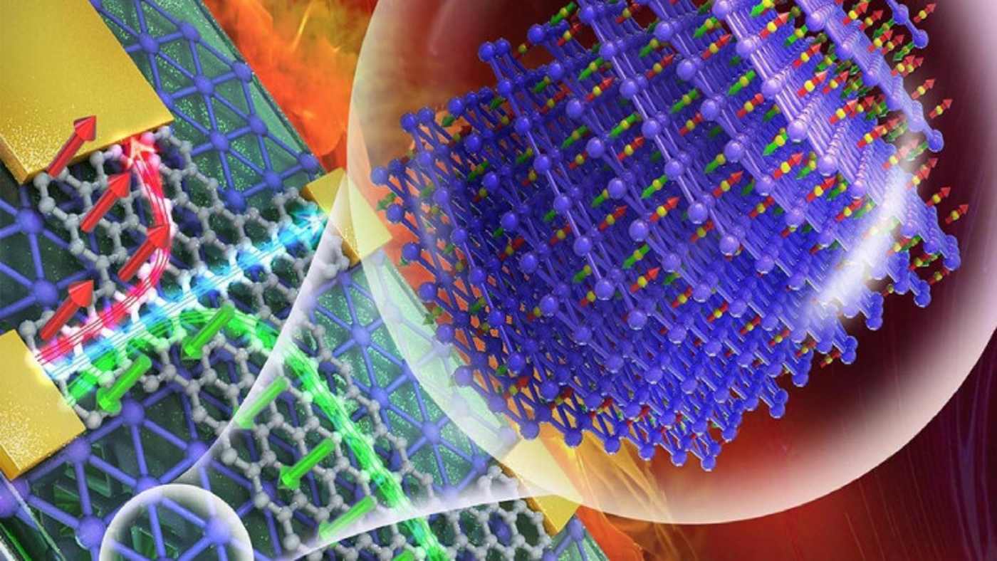
A constant current is required to form this binary, but Dowben and his colleagues have created a new transistor that creates this binary using “spin” to dictate whether a terminal reads a 1 or a 0. Spin is a magnetism-related property of electrons that points either up or down.
They swapped silicon for a robust material called graphene, which can be as thin as one molecule thick. Then they lined it with chromium-oxide, a magneto-electric material, which means that electrons on its surface can be flipped to spin up or down based on the application of a meager amount of current.
Applying positive voltage causes the electrons’ spin to flip them up, while a negative charge flips them down.
“This potentially gives you huge fidelity at very little energy cost,” Dowben explains to his university press. “All you did was apply voltage, and it flipped.” Dowben explained that there are other materials that can be overlaid with chromium, not just graphene, and entrepreneurs and designers will all begin, now that the demonstration of a post-silicon transistor has been shown to be superior, try to find the optimal material.”
Moving forward
“Now that it works, the fun begins, because everybody’s going to have their own favorite 2D material, and they’re going to try it out,” Dowben said. “Some of them will work a lot, lot better, and some won’t. But now that you know it works, it’s worth investing in those other, more sophisticated materials that could.
“Now everybody can get into the game, figuring out how to make the transistor really good and competitive and, indeed, exceed silicon.”
MORE: French Town to Light its Streets With Bacteria Luminescence That Needs No Electricity
The team received support from the National Science Foundation’s Established Program to Stimulate Competitive Research, which funded the $20 million Emergent Quantum Materials and Technologies collaboration at Nebraska.
Replacing the silicon transistor is like replacing the backbone of the computing revolution. What comes next, whether graphene or something else, means that we will be moving into a totally new paradigm.
POWER UP the Good News; Share This Article…


